Abhiyantha Training Program

Mastering VLSI Analog Layout
From Concepts to Industry Readiness

Start Date: Oct 14, 2026 | Mode: Hybrid


Register Now

Program Overview

Program Description


This Analog Layout Skill Development Program is designed to prepare learners for industry-ready roles in Analog and Mixed-Signal VLSI by imparting both foundational principles and practical layout skills.


Learners will master the techniques and tool-flows used by Analog Layout Engineers, moving from basic device layout through to advanced optimization under real-world constraints.

Key Highlights

  • Gain a strong foundation in Analog layout, emphasizing device matching, parasitic management, & noise optimization

  • Learn floorplanning, power routing, and substrate connection techniques essential for reliable Analog chip design.

  • Build hands-on expertise in DRC, LVS, and PEX verification flows, along with post-layout simulation and performance optimization.

  • Master advanced layout practices like common-centroid design, guard rings, low-power techniques, and corner variation handling.

Why Abhiyantha

VLSI professionals

Expert Guidance

Learn from seasoned professionals and Cadence Certified Trainers

VLSI professionals

Hands-on Experience

Master industry-standard tools through practical, real-world exposure

VLSI professionals

Industry-Oriented Projects

Strengthen your skills with project-based learning tailored to industry needs

VLSI professionals

Industry-Recognized Certificate

Earn a globally recognized certificate


Why Abhiyantha's Analog Program?

Master Core Layout Design Skills

Get trained in Analog layout fundamentals

Aligned with Industry Demands

Cadence Virtuoso & industry workflows

Capstone Project

End-to-end Analog block design

Accelerated Career Progression

Strong fundamentals, less competitors

Program Outline

  • VLSI and Semiconductor Fundamentals
  • MOSFET Fundamentals and Device Characteristics
  • CMOS Inverter and Digital Logic Design
  • CMOS Fabrication and Design Rules
  • VLSI Layout Fundamentals
  • Standard Cell Architecture and Layout
  • Combinational and Sequential Cell Layout
  • DRC, LVS and Physical Verification
  • Standard Cell Library and Basic Physical Integration

  • Fundamentals of Analog Layout
  • Analog Layout Challenges and Design Considerations
  • Multi-Finger Devices and Diffusion Sharing
  • Matching Techniques and Symmetry
  • Common Centroid and Interdigitation
  • Current Mirror Layout
  • Differential Pair and OTA Layout
  • Resistor and Capacitor Layout
  • Guard Rings, Substrate Contacts and Shielding
  • DRC, LVS and Parasitic Extraction

  • Two-Stage Op-Amp Layout
  • Compensation and Critical-Net Routing
  • Bandgap Reference Layout
  • Comparator and LDO Layout
  • Level Shifter Layout
  • Analog Block Integration
  • Post-Layout Simulation and Parasitic Analysis
  • Matching, Symmetry and Reliability Considerations
  • Analog Layout Review and Sign-Off

  • Memory Architecture and Layout Fundamentals
  • 6T SRAM Bitcell Layout
  • SRAM Array and Tiling
  • Row and Column Periphery
  • Sense Amplifier and Write Driver Layout
  • Decoder and Wordline Driver Layout
  • Memory Block Integration
  • Hierarchical Layout and Block Assembly
  • Power Planning and Pin Integration
  • Hierarchical DRC/LVS and Parasitic Verification

Industry Tools & Expert Trainer

Industry-Standard EDA Tools* - Cadence

  • Virtuoso
    Custom IC design platform for Analog, RF circuits
  • Spectre
    High-performance Analog simulator for circuit simulation
  • PVS/Pegasus
    Physical verification system for design rule checking
  • Quantus
    Extraction solution for accurate parasitic extraction
  • ADE Assembler
    Environment for simulation setup and analysis
  • SKILL IDE
    Development environment for SKILL programming
Note: Participants will receive a total 100+ hours of online tool access.

Learn from Cadence Certified Experts

Mr. VDK
Mr. Venugopal D Kulkarni
Domain Expert


32+ years of combined academic and industry experience in Analog & Mixed-Signal IC Design and Electronic System Design
M.Tech (IIT Bombay), B.E. (Karnataka Univ.) with expertise in Analog & Mixed-Signal design.
Chief Mentor, Entuple Technologies, driving advanced Analog & Mixed-Signal IC training.
Trained 3000+ engineers in IC design, system modeling, and electronic system design.

.

Mr. Shiva Prasad B K
Technical Expert
Cadence Certified Instructor
10+ years of industry experience in VLSI design and training
M.Tech in VLSI Design with specialization in Analog Circuits
Certified Cadence instructor with extensive teaching experience
Expert in Analog and Mixed-Signal IC design methodologies
Passionate about mentoring next-generation VLSI engineers

Program Details

October 14, 2026

Timings: 6:30 PM to 8:30 PM

Learning Mode : Hybrid Mode

Live and interactive learning

Duration
4 Months
( 1 Month Offline & 3 Months Online)

Comprehensive training program

Recordings

Access to all the session recordings


Certificate
Industry Recognized

Upon successful completion

Pre-requisites
  • Students and Graduates in ECE/EEE or related streams
  • Faculty and Research Scholar

Course Fee

Choose the plan that works best for you

Mastering VLSI Analog Layout

₹ 75,000 + GST
₹ 49,999 + GST
Register Now

Talk to us!

Phone: 93539 01711/89519 24075 | Email: training@abhiyantha.com

What Our Students Say

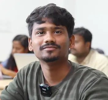
trupthi

I joined Abhiyantha, in July 2023. I had a great experience at Abhiyantha. I was trained by great industry experts in which I had experience with hands-on learning and deep learning knowledge, which led me to explore emerging trends in the VLSI industry. I was recently placed at Cadence Design Systems by Abhiyantha. I thank Abhiyantha for their constant support and guidance till the completion of my training.".

Trupti Hawaldar

Career Builder Student

Saket Jadhav

Abhiyantha course offered expert training in Synthesis, Timing Analysis, and Physical Design with hands-on projects and Cadence tools. The industry guidance and placement support significantly advanced my VLSI career. Grateful for the opportunity.

Saket Jadhav

Career Builder Student

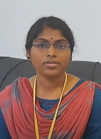
Kavimalar K,

Driven by my passion for VLSI, I was guided by Abhiyantha, The supportive technical team and their step-by-step approach, enriched with real-world examples, made complex VLSI concepts clearer. This internship provided invaluable industry exposure and significantly enhanced my skills. A big thank you to Abhiyantha for this transformative experience!".

Kavimalar K,

Internship Student, GCE Thanjavur, TN

Vikas Madanashetti

I enrolled in the Physical Design and Verification course organized by Abhiyantha, I acquired extensive knowledge in various areas such as basic digital verification with Verilog, synthesis, static timing analysis, and both physical design and verification. The course also provided hands-on experience with tools including Xcelium, Genus, Tempus, Innovus, Pegasus, and Voltus. In addition, it covered soft skills training and personal branding, including LinkedIn, critical thinking, and mock interviews. I want to extend my gratitude to all the trainers at Abhiyantha for their invaluable support."

Vikas Madanashetti,

Career Builder Student

Ready to Start Your Analog VLSI Journey?